YANG Jia-shi, ZHOU Hong-gang. Interface waves between two piezoelectric half-spaces with a semiconductor film[J]. Journal of Zhejiang University Science A, 2005, 6(2): 90-96.
@article{title="Interface waves between two piezoelectric half-spaces with a semiconductor film", author="YANG Jia-shi, ZHOU Hong-gang", journal="Journal of Zhejiang University Science A", volume="6", number="2", pages="90-96", year="2005", publisher="Zhejiang University Press & Springer", doi="10.1631/jzus.2005.A0090" }
%0 Journal Article %T Interface waves between two piezoelectric half-spaces with a semiconductor film %A YANG Jia-shi %A ZHOU Hong-gang %J Journal of Zhejiang University SCIENCE A %V 6 %N 2 %P 90-96 %@ 1673-565X %D 2005 %I Zhejiang University Press & Springer %DOI 10.1631/jzus.2005.A0090
TY - JOUR T1 - Interface waves between two piezoelectric half-spaces with a semiconductor film A1 - YANG Jia-shi A1 - ZHOU Hong-gang J0 - Journal of Zhejiang University Science A VL - 6 IS - 2 SP - 90 EP - 96 %@ 1673-565X Y1 - 2005 PB - Zhejiang University Press & Springer ER - DOI - 10.1631/jzus.2005.A0090
Abstract: In this work propagation of anti-plane (SH) waves in two piezoelectric ceramic half-spaces with a thin layer of a semiconducting material between the half-spaces is studied, and waveattenuation and dispersion caused by semiconduction as well as wave amplification by a biasing electric field are examined.
Darkslateblue:Affiliate; Royal Blue:Author; Turquoise:Article
Article Content
. INTRODUCTION
Piezoelectric materials are either dielectrics or semiconductors (Auld, 1973). An acoustic wave propagating in a piezoelectric crystal is usually accompanied by an electric field. When the crystal is also semiconducting, the electric field produces currents and space charge resulting in dispersion and acoustic loss (Hutson and White, 1962). The interaction between a traveling acoustic wave and mobile charges in piezoelectric semiconductors is called acoustoelectric effect which is a special case of a more general phenomenon called wave-particle drag (Weinreich et al., 1959). It was found that an acoustic wave traveling in a piezoelectric semiconductor can be amplified by the application of a dc electric field (White, 1962). This phenomenon is called acoustoelectric amplification of acoustic waves. The acoustoelectric effect and amplification of acoustic waves can also be achieved in composite structures of piezoelectric dielectrics and nonpiezoelectric semiconductors (Dietz et al., 1988). In these composites the acoustoelectric effect is due to the combination of the piezoelectric effect and semiconduction in each component phase. The acoustoelectric effect and acoustoelectric amplification of acoustic waves have led to the development of acoustoelectric devices (Dietz et al., 1988; Kino, 1976; Heyman, 1978; Busse and Miller, 1981). Both surface acoustic waves (SAW) and bulk acoustic waves (BAW) have been used for acoustoelectric devices. The basic behavior of piezoelectric semiconductors and the acoustoelectric effect can be described by a linear phenomenological theory (Hutson and White, 1962; White, 1962). More sophisticated nonlinear theories for deformable semiconductors had also been developed (de Lorenzi and Tiersten, 1975; Maugin and Daher, 1986). Due to multi-field coupling and anisotropy, device modeling by these theories presents complicated mathematical problems. Exact analysis is possible only in rare cases, e.g., the one-dimensional problem of thickness vibrations of plates (Wauer and Suherman, 1997). In this work we study the propagation of anti-plane waves near the interface between two piezoelectric ceramic half-spaces with a thin layer of a nonpiezoelectric semiconductor between them. Following a summary of the three-dimensional equations of linear piezoelectric semiconductors, two-dimensional equations for a thin piezoelectric semiconductor film are given to model the semiconductor layer. Propagation of anti-plane waves under a dc field is then analyzed. Frequency equations that determine the dispersion relations are obtained. An approximate analytical solution of the frequency equations and numerical results are presented. Finally, some conclusions are drawn.
. THREE-DIMENSIONAL EQUATIONS
Consider a homogeneous, one-carrier piezoelectric semiconductor under a uniform dc electric field . The steady state current is . The conventional summation for repeated tensor indices is used. When an acoustic wave propagates through the material, perturbations of the electric field, the carrier density and the current are denoted by Ej, n and Ji. The linear theory for small signals involves the equations of motion, Gauss’s law, and the principle of conservation of charge (Hutson and White, 1962; Wauer and Suherman, 1997): where a comma followed by an index denotes partial differentiation with respect to the coordinate associated with the index. A superimposed dot represents differentiation with respect to time. The above equations are accompanied by the following constitutive relations (White, 1962) where
With successive substitutions form Eqs.(2) and (3), Eq.(1) can be written as three equations involving u, ϕ and n
On the boundary of a finite body with a unit outward normal ni, the mechanical displacement ui, the traction vector Tijni, the electric potential ϕ, the normal component of the electric displacement vector Dini, the carrier density n and the normal current Jini may be prescribed on the boundary of a finite body (Wauer and Suherman, 1997).
. EQUATIONS FOR A THIN FILM
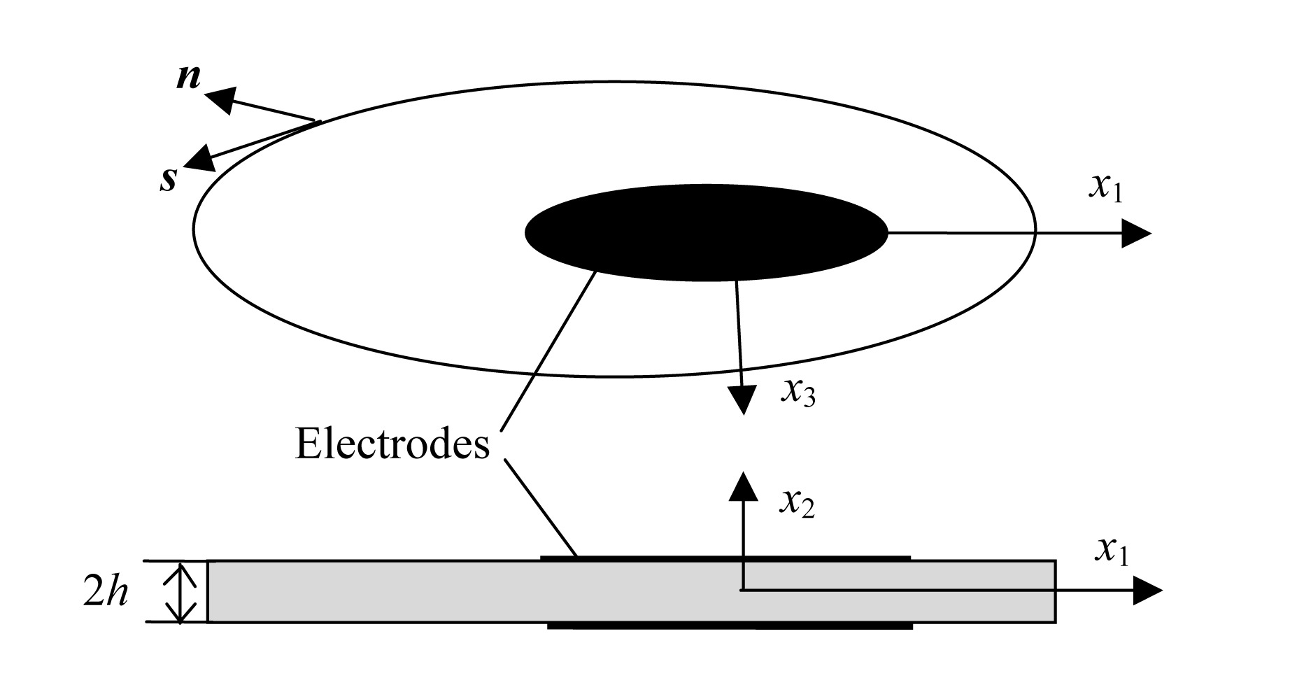
Consider a piezoelectric semiconductor film of thickness 2h as shown in Fig.1 with the coordinate system. The film is assumed to be very thin. We need a two-dimensional theory for the film in the manner of the equations for generalized plane stress in elasticity (Sokolnikoff, 1956). The dominating stress components of this film are T11, T33 and T13. We make the usual stress relaxation
Fig.1 Plan view and cross section of a thin film of piezoelectric semiconductor
According to the compact matrix notation (Tiersten, 1969a), with the range of p as 1, 2, …, and 6, Eq.(5) can be written as
For convenience we introduce a convention that subscripts u, v, w take the values 2, 4, 6 while subscripts r, s, t take the remaining values 1, 3, 5. Then Eq.(2)1,2 can be written as where Eq.(6) has been used. From Eq.(7)2 we have
Substitution of Eq.(8) into Eq.(7)1,3 yields the mechanical and electric constitutive relations for the film
whose material constants are
We now introduce another convention that subscripts a, b, c and d assume 1 and 3 but not 2. Then Eq.(9) can be written as
Integrating the equations in Eq.(1)1 for i=1, 3 and Eq.(1)2,3 with respect to x2 through the film thickness, we obtain the following two-dimensional equations of motion, Gauss’s law and the conservation of charge: where ua, Tab, Da, Ja and n are averages of the corresponding three-dimensional quantities along the film thickness.
. INTERFACE WAVES
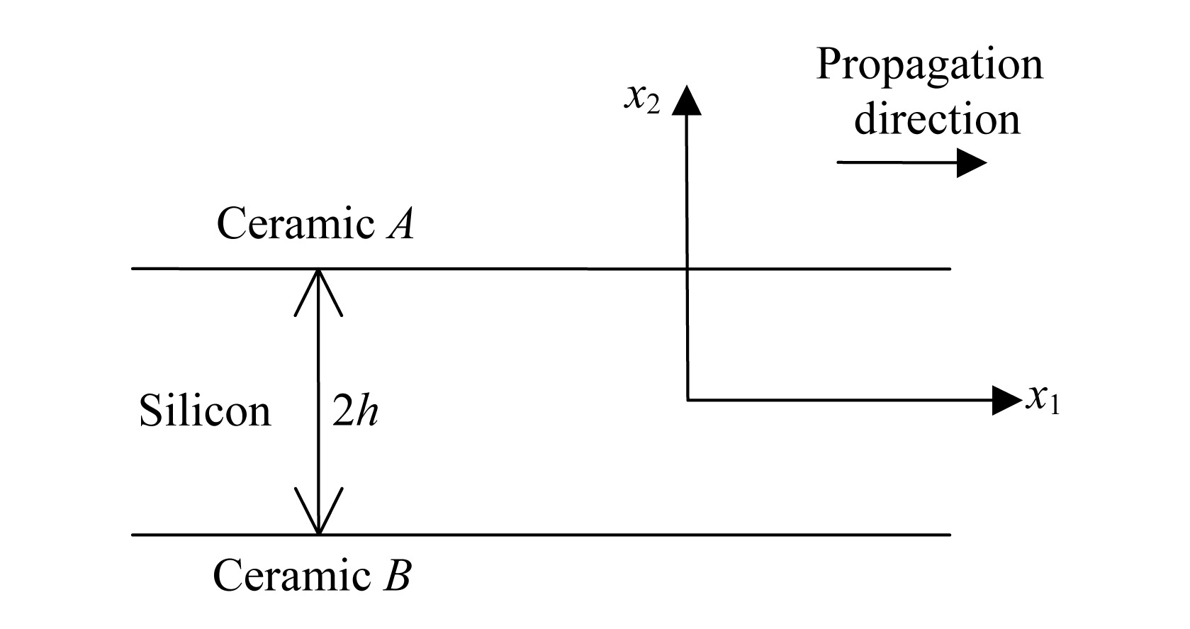
Consider two piezoelectric half-spaces of polarized ceramics with a semiconductor film of silicon between them (Fig.2). Silicon is a cubic crystal with m3m symmetry and without piezoelectric coupling. The film is assumed to be very thin as compared to the wavelength we are interested in, and can be modeled by the film equations in the previous section. In this case the equations of the thin film will appear as interface continuity conditions between the half-spaces. This type of approximation had been used to model surface waves guided by thin elastic films (Tiersten, 1969b). For ceramics poled in the x3 direction we have where c66=(c11–c12)/2 (Tiersten, 1969a). We are interested in anti-plane motions with (14)
Fig.2 Two ceramic half-spaces with a semiconductor film
The non-vanishing strain and electric field components are where is the two-dimensional gradient operator. The nontrivial components of Tij and Di are (16)
The nontrivial components of the equations of motion and charge take the following form: (17) where ∇2 is the two-dimensional Laplacian . Introducing (Bleustein, 1968)
then
and where (21)
. Fields in the upper half-space
For the upper half-space, the solution can be written as where U and ΨA are undetermined constants,
and (24)
For continuity conditions, we need ϕA, T23 and D2 in ceramic A. We denote T23 and D2 by TA and DA:
. Fields in the lower half-space
Similarly, for the lower half-space, the solutions can be written as where (28)
Note that the continuity of u between the two half-spaces is already satisfied. For the other continuity conditions, we need ϕB, T23 and D2 in ceramic B. We denote T23 and D2 by and DB: (28)
. Fields in the film
For long waves, fields in the semiconductor film can be treated as functions of x1 and time only. Denote the fields in the film by where Φ and N are undetermined constants. Eq.(30) already satisfies the continuity of mechanical displacement between the film and the ceramic half-spaces. We use a prime to indicate the elastic and dielectric constants as well as the mass density of the film. The elastic and dielectric constants are given by ,
Consider the case when the dc biasing electric field is in the x1 direction. From Eqs.(30), (31), (11) and (2)3 we obtain
. Continuity conditions
From the continuity of the electric potential and Eq.(12), we have
Eq.(33) is a system of linear homogeneous equations for U, ΨA, ΨB, and N. For nontrivial solutions the determinant of the coefficient matrix of Eq.(33) has to vanish, which gives the following frequency equation that determines the dispersion relations of the waves:
Or, in terms of the wave speed v, Eq.(34) can be written as where (36)
(i) As a special case, when h=0, i.e., the semiconductor film does not exist, Eq.(35) reduces to the equation that determines the speed of interface waves between two ceramic half-spaces (Maerfeld and Tournois, 1971);
(ii) Different from the interface waves (Maerfeld and Tournois, 1971) which are not dispersive, waves determined by Eq.(35) are dispersive due to the presence of the film which introduces a length parameter h into the problem;
(iii) If the two half-spaces are of the same ceramics with opposite poling directions, we have (Maerfeld and Tournois, 1971) , ,
Eq.(38) represents a dispersive but nondissipative wave. In this case the electric fields produced by the two ceramic half-spaces cancel with each other in the semiconductor film. Hence there is no conduction and dissipation in the film.
(iv) If the two half-spaces are of the same ceramics with the same poling direction, Eq.(35) reduces to
The denominator of the right-hand side of Eq.(40) indicates that a complex wave speed may be expected and that the imaginary part of the complex wave speed may change its sign (wave amplification) when changes its sign or
i.e., the acoustic wave speed is equal to the carrier drift speed.
. NUMERICAL RESULTS
For numerical results we consider Eq.(40). When semiconduction is small, Eq.(40) can be solved by an iteration or perturbation procedure. As the lowest (zero) order of approximation, we neglect the semiconduction and denote the zero-order solution by v(0). Then from Eq.(40) (42)
which determines v(0). For the next order we substitute v(0) into the right-hand side of Eq.(40) and obtain the following equation for v(1)
which suggests a wave that is both dispersive and dissipative.
For the ceramic half-spaces consider PZT-5H with ρ0=7500 kg/m3 and (Auld, 1973)
c11=12.6, c33=11.7, c44=2.30,
c12=7.95, c13=8.41×10¹⁰ N/m2,
e15=17.0, e31=−6.5, e33=23.3 C/m2,
ε11=1700ε0, ε33=1470ε0, ε0=8.854×10⁻¹² farads/m
For silicon with ρ0=2332 kg/m3, we have (Hellwege and Hellege, 1979; Lide, 2001-2002)
The mobility of electrons and holes of silicon at 300 °K are (Navon, 1986)
The diffusion constants can be determined from the Einstein relation (Navon, 1986) where T is the absolute temperature, and k the Boltzmann constant. At room temperature kT/qe= 0.026 V (Navon, 1986) where qe=1.602×10⁻¹⁹ coulomb is the electronic charge.
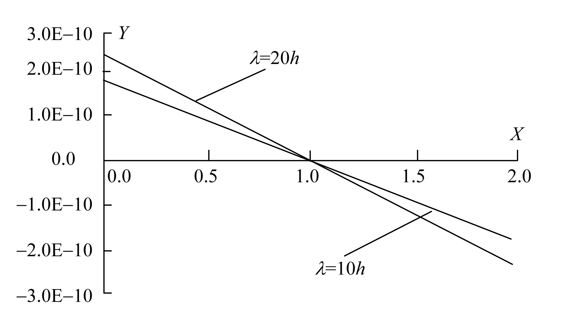
We plot the real parts of v(0) and v(1) versus ξ in Fig.3. The dimensionless wave number X and the dimensionless wave speed Y of different orders are defined by
Fig.3 Dispersion relations
γ is a dimensionless number given by (49)
which may be considered as a normalized electric field. It represents the ratio of the electron drift velocity and the speed of the shear acoustic wave. Because of the use of the thin film equations for the semiconductor layer, our solutions are valid only when the wavelength is much larger than the film thickness (X<<1). It can be seen that semiconduction causes dispersion. This conduction induced dispersion varies with the dc biasing electric field.
Fig.4 shows the imaginary part of v(1) versus X=γ. λ=2π/ξ is the wave length. The dimensionless number describing the decaying behavior of the waves is defined by
Fig.4 Dissipation as a function of the dc bias
When the dc bias is large enough (approximately γ>1), the decay constant becomes negative indicating wave amplification. The transition from damped waves to growing waves indeed occurs when Eq.(41) is true for v(0). These agree qualitatively with the behavior of the 1-D plane waves (White, 1962).
. CONCLUSION
Dispersion relations for anti-plane interface waves between two piezoelectric ceramic half-spaces with a semiconductor film are obtained. It is shown that semiconduction causes dispersion and acoustic loss in these waves. Acoustoelectric amplification occurs when the electron drift speed under a dc bias is larger than the shear acoustic wave speed. The equations for thin films simplify the analysis.
Acknowledgements
The second author, with a B.S. and an M.S. from Zhejiang University, takes this opportunity to thank his Alma Mater.
References
[1] Auld, B.A., 1973. Acoustic Fields and Waves in Solids, John Wiley and Sons, New York,:357-382.
[2] Bleustein, J.L., 1968. A new surface wave in piezoelectric materials. Appl Phy Lett, 13:412-413.
[3] Busse, L.J., Miller, J.G., 1981. Response characteristics of a finite aperture, phase insensitive ultrasonic receiver based upon the acoustoelectric effect. J Acoust Soc Am, 70:1370-1376.
[4] de Lorenzi, H.G., Tiersten, H.F., 1975. On the interaction of the electromagnetic field with heat conducting deformable semiconductors. J Math Phys, 16:938-957.
[5] Dietz, D.R., Busse, L.J., Fife, M.J., 1988. Acoustoelectric detection of ultrasound power with composite piezoelectric and semiconductor devices. IEEE Trans on Ultrasonics, Ferroelectrics, and Frequency Control, 35:146-151.
[6] Hellwege, K.H., Hellege, A.M. .(.E.d.s.)., 1979. Landolt-Bornstein, Numerical Data and Functional Relationships in Science and Technology, Springer-Verlag, New York,:266
[10] Maerfeld, C., Tournois, P., 1971. Pure shear elastic surface waves guided by the interface of two semi-infinite media. Appl Phys Lett, 19:117-118.
[11] Maugin, G.A., Daher, N., 1986. Phenomenological theory of elastic semiconductors. Int J Engng Sci, 24:703-731.
[12] Navon, D.H., 1986. Semiconductor Microdevices and Materials, CBS College Publishing, New York,:
[13] Sokolnikoff, I.S., 1956. Mathematical Theory of Elasticity, McGraw-Hill, New York,:
[14] Tiersten, H.F., 1969. Linear Piezoelectric Plate Vibrations. , Plenum, New York, :


Open peer comments: Debate/Discuss/Question/Opinion
<1>